
Now that I’ve built a small 8086 based system – there’s something I’ve been wanting to do for a while: Acquire a K1810BM86 and run it.
I first saw one of these at a Soviet technology museum a number of years ago and was fascinated. I had no idea that the USSR had developed the means to produce fairly complex microprocessors. Needless to say, I had to own one.
I had read a number times around the internets that it is electrically and binary compatible with the first 5MHz Intel parts, but is this completely true? Now I can personally find out with ease. One of the first things I had noticed, even before I bought one, is that it appears a little smaller than the genuine article, but it appeared that this was just the plastic casing. Turns out I was wrong.
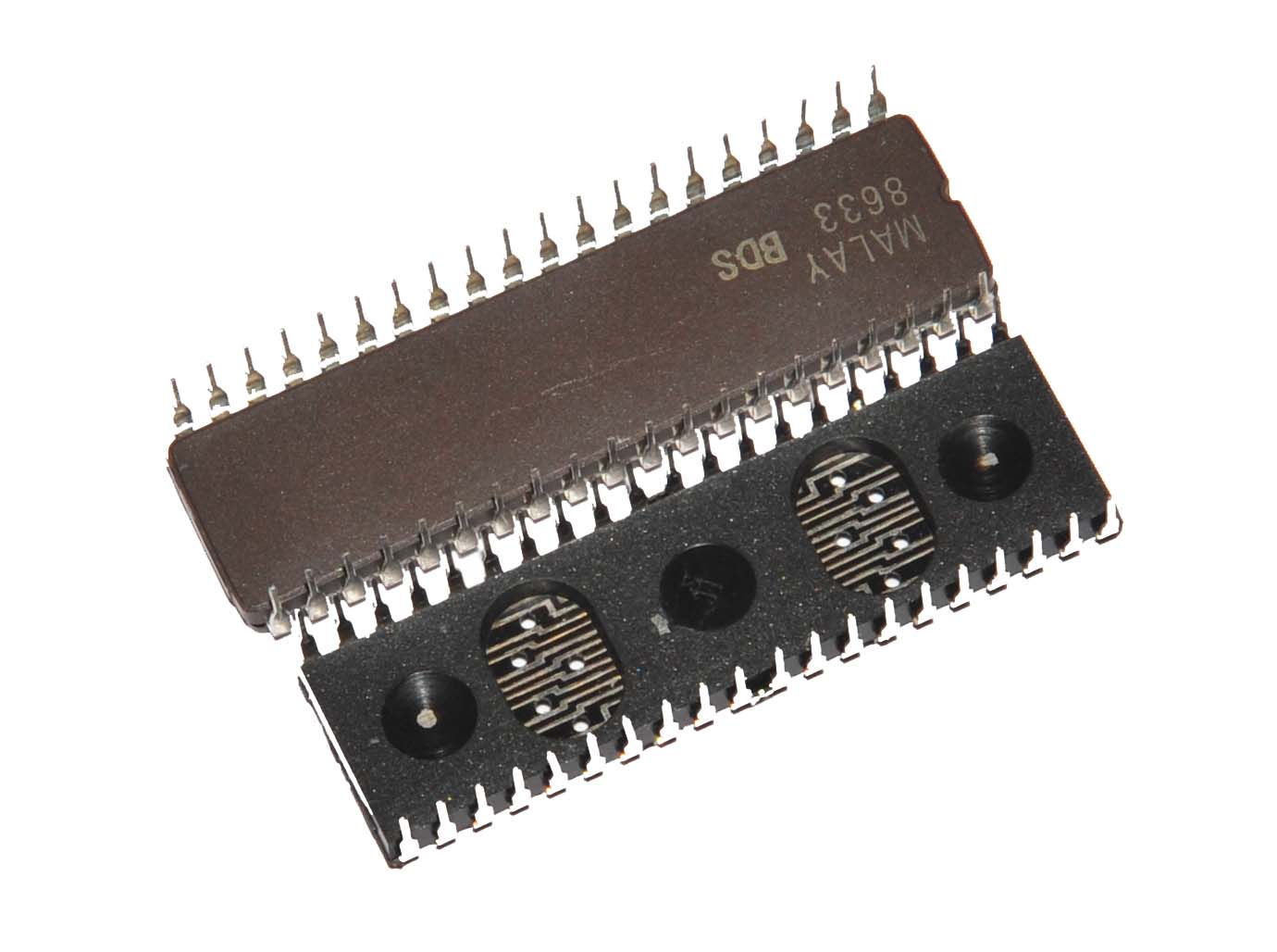
Oh dear. It appears that K1810VM86 has been packaged not with the usual imperial 0.1″ (2.54mm) pin spacing, but instead a metric 2.50mm, so it doesn’t fit into the 0.1″ sockets I’m using, nor can I obtain the correct socket. What a freaking pain.
But it turns out, there is a simple solution:

A cheap “wipe” IC socket, which has a little lengthwise slide room.
One certainly has to be careful with these chips, as those cuts in the packaging make them fragile, like a KitKat bar. Which brings me to the next thing I wondered, why the bizarre packaging?

There’s plenty of conjecture around various forums as to the reason for this style i.e. to make it look cool or to save plastic, but I don’t think any of this is likely. The chip on the left eliminates both of those theories.
Both of these appear to have been injection moulded at two points from the underside, which would likely mean that it’d be necessary to have a couple of ridges in the top of the mould to stop the traces from being torn from the die, or even the whole lot from squashed up into the top of the mould. In the case of the one of the right, a larger area restraining the traces likely means an even more stable moulding process.
If all of this is true, the strange appearance is more a result of a crude packaging process than any other more interesting explanation.
But anyway. The more important question: Do these actually work?
Yep. All three samples I have work perfectly, but like pretty much any 8086 I’ve tried, don’t overclock much more than a single megahertz. Interestingly they do run quite a lot cooler than the original NMOS 8086.
In conclusion: There some something supremely satisfying about writing code to execute on a communist processor.
Nice work! I was working with this IC during my university studies
>Which brings me to the next thing I wondered, why the bizarre packaging?
Actually it’s a surface-mount package embedded into DIP adapter. There were several grades of soviet ICs, one of which is military and space grade (Acceptance level 5 and 9), and it required ceramic or other protective package, high temp and radiation tolerance, gold coated pins in special configurations and some other differences. It seems that chips that could not fit this acceptance level were repackaged into more common DIP package and sold as civil ones
http://upload.wikimedia.org/wikipedia/commons/thumb/1/16/Eprom.jpg/640px-Eprom.jpg?uselang=ru
Печально, что в 90-х микроконтроллеры и технологии имеющиеся в СССР были просто уничтожены, на данный момент всё выглядит не очень хорошо, тех процесс так же и остался около 100 нанометров, однако могут ввести новые заводы на 65 нанометров, если будут покупатели электроники из РФ, на данный момент есть только ЦП от Ангстрема и МЦСТ…
http://www.mcst.ru/ – тут можно посмотреть характеристики
CPU – 1891ВМ7Я
Core – 2
MhZ – 500 – 900
Rough translation:
Unfortunately during the 1990’s development of microcontrollers and similar technology in the USSR was laid to waste. Even today, things haven’t improved much. Semiconductor fabrication processes have remained around 100 nanometers, but plans are on the horizon to introduce new plants with 65 nanometer processes.
As for any remaining would-be buyers of technology developed in Russia, they’ll have to be happy with just the one CPU from Angstrom and MCST.
Known as “1891ВМ7Я”, it’s dual core, and runs between 500 and 900MHz.
Your project is really cool!
BTW these Soviet\Russian-made ICs are still for sale here for about $1,35/piece, geeks are welcome.
Greetings from St.Petersburg, Russia )
Because the world is metric. 200 years ago the whole world agreed to use SI units such as meter and kilogramms. Bizarre is to introduce chips in imperial units at all. Shame on this decision. There are always people in the world that think they are something better and must do it in a different way. The problems of the world can only be solved together and that means to have the discipline to accept agreements. Therefore I see no room for imperial units.