Recently I started looking into the next phase of development I wanted to do on 8OD, specifically, to make a bus available on the 36-pin header and start attaching peripherals to it.
As I looked back through the design, something jumped out at me…
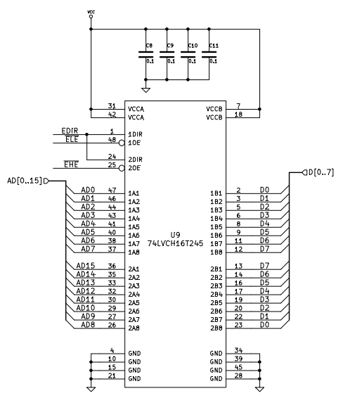
U9 is a not-entirely-necessary, but nice to have bit of logic which performs bus steering, to make the addressing of 8-bit peripherals easier. It is effectively a bus transceiver, although not quite performing the same role as an actual bus transceiver.

Yet…
The signals made available on the 8086 for the control of bus transceivers, are N.C. Well well…
Diving back in the the CPLD’s VHDL code, I can see that I’ve derived the control signals for U9 from the 8086’s bus control signals, not the dedicated transceiver control signals. This of course is less than ideal, but is it actually a problem? Let’s get those timing diagrams out and have a look.

First stop, the 8086 read timings. Straight away, it doesn’t look good. Because the #OE’s of the transceiver are asserted for the period of the #CS signals of the two peripherals behind it, the de-assertion of #RD will reverse the direction of the transceiver while it is still driving the bus.
Therefore the above diagram shows that this inappropriate use of RD# causes a potential bus clash between peripherals and the transceiver (U9), whereas DT/#R (Not used by my design) is well clear of any such eventualities. How the heck did I miss that?
But as previously stated, this only highlights a potential clash. Because the peripheral is assumed to be driving the bus during this period, we have to examine it to determine if there is an actual clash. Let’s take a look at the SC16C554 datasheet:

That’s not good, it’s now very likely that there is a clash. In terms of the UART (U10), this is clearly represented and quantifiable by the symbol ‘t12h’.

Which is 15 nanoseconds per bus cycle.
The only remaining hope lies within the propagation times of U9 (SN74LVC16T245). I’ve got a pretty good feeling there isn’t going to be any good news there either.
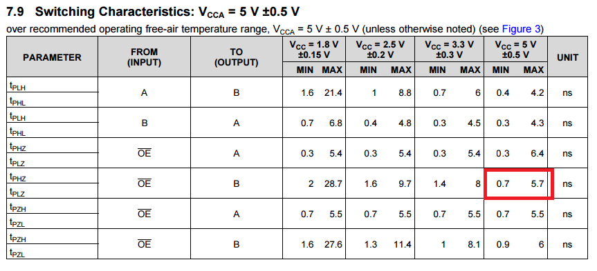
And there it is. U9 can change direction significantly faster than U10 can release the bus. There’s officially a major problem with my design.
I’m a little miffed about this. I really thought the 8OD.1 board was free of mistakes, certainly, it didn’t show any problems during my testing. In some respects, what I’ve just found is the worst kind of problem, as it is likely to be missed during design verification, and will lead to premature failure, after the product has been shipped.
It’s just as well I didn’t mass produce these things.
So what next?
 Wire mods.
And a couple of pull-up resistors. This time I checked the need for these carefully, as I was keen not to get my backside kicked by yet another quirky detail, specifically that control signals tend to float during certain periods, i.e. Hold Acknowledge, Reset.
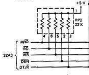 And there they are on the original SDK-86 schematic, circa 1978.
I’ve now got DT/#R connected to the DIR signals on U9, and #DEN to the CPLD to control the #OE signals for U9. This is fairly faithful to the original guidelines, and will make these boards reliable in the long term.
So now I’ve got to revise the board. I guess this isn’t such a bad thing, as there’s already a list of things I want to improve with the current design.
Moral of the story
8OD’s 8-bit bus spur was a design annoyance, which I didn’t put as much thought into as I should have. As is always the case when designing complex electronics: If you haven’t thought of absolutely everything, there will always be a major problem hiding in the overlooked details.
Posted in Vintage microcontrollers